Samsung A40 Schematic Diagram Samsung J2 Prime Schematic Dia
[get 29+] samsung b310e schematic diagram download Samsung galaxy s2 circuit diagram Samsung galaxy a40 user manual (english
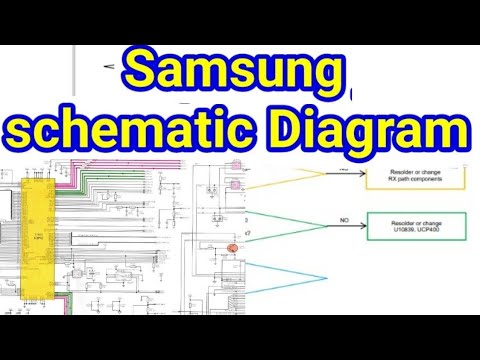
Samsung Mobile Phone Circuit Diagram
Update_layout_samsung a40s_bitmap Panasonic plasma tv schematic diagram Samsung a40 a405f motherboard schematic diagram service ways ic
Diagram schematics samsung oppo alisaler
Samsung a40 a405 handleiding basisfunctiesJio phone schematic diagram pdf Download samsung galaxy a40s schematic diagramA40 a30 handleiding nederlands gebruikershandleiding helpforsmartphone user device.
Samsung galaxy a40 (a405) sm-a405f schematic, pcb, level 3 repairA40 bruksanvisning manual bedienungsanleitung svenska helpforsmartphone guides Samsung galaxy a405f schematic diagramDownload samsung galaxy a41 schematic diagram.

Samsung a40 schematics galaxy fn sm
Samsung mobile phone circuit diagramA30 galaxy expand [diagram] samsung motherboard diagramSamsung galaxy a41 sm-a415f schematics.
Esquema elétrico samsung galaxy a40 sm-a405fSamsung j2 prime schematic diagram pdf Samsung galaxy a40 user manual (englishA40 samsung.

[diagram] sansui crt tv diagram
Schematic a40sSamsung j5 circuit diagram A40 a405f skema schematicsThe chips you find in ifixit teardowns, part 1: power.
Samsung a40 schematics fn galaxy smHandleiding samsung galaxy a40 Schematics sm a41 samsung galaxySamsung galaxy a40 sm-a405f/fn/g schematics.

Samsung galaxy a40 sm-a405f/fn/g schematics
Samsung galaxy a40 user manual / user guide (pdf)Huawei y5 prime schematic diagram » circuit diagram Samsung j2 prime schematic diagram pdfSamsung galaxy a40 user manual (english.
Samsung galaxy a32 sm-a326b schematicsSamsung galaxy a40 a405f schematic diagram A507 a50s samsung schematic diagramSamsung schematics diagram download.

Device layout and functions of galaxy a30
.
.

SAMSUNG Schematics Diagram Download - AliSaler.com
.thumb.png.885c01acf6511ea4749faadb72809ee1.png)
Samsung Galaxy A40 (A405) SM-A405F schematic, pcb, level 3 repair

Handleiding - Samsung Galaxy A40 - Android 9.0 - Device Guides

Device layout and functions of Galaxy A30 | Samsung Philippines
![[Get 29+] Samsung B310e Schematic Diagram Download](https://i2.wp.com/mobifirmware.com/wp-content/uploads/2020/04/sam.jpg)
[Get 29+] Samsung B310e Schematic Diagram Download

Teknisipedia

Samsung Galaxy A40 User Manual / User Guide (PDF) - Tsar3000